PRODUCTS
biRAPID
GaN 3 Phase Inverter
HGCB-6B-401120
GaN Inverter for MHz class high frequency switching
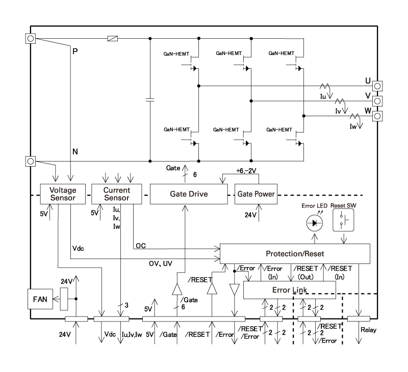
6 unit of GaN Systems’ GaN E-HEMT are used to form a Three-Phase full-bridge inverter 3 phase full bridge inverter. An A5 size that capable of max. 5MHz switching frequency operation. Embedded with sensors that allow the Voltage/Current feedback. Can be operated as Chopper circuit or Single Phase inverter too.
GaN Inverter for MHz class high frequency switching
Operational up to 5MHz
Can be used just by preparing of 24V/5V power source,
cabling and a set of controller.
Open Concept Design
Suitable for a various testing.
Circuit diagram is provided as a design reference.
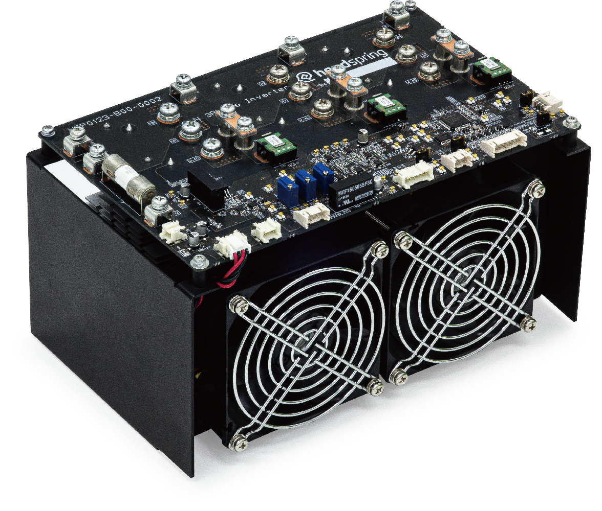
Specification (Model: HGCB-6B-401120)
| Equipment size | W:209mm / D:134mm / H:120mm | Excluding protrusions |
|---|---|---|
| Mass | 1.9kg | |
| DC voltage range | 0V~400V | P-N terminal voltage |
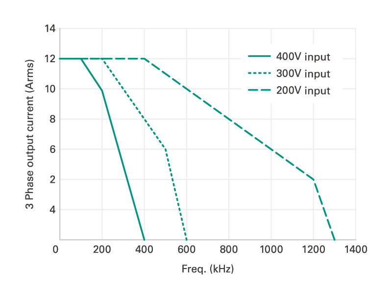
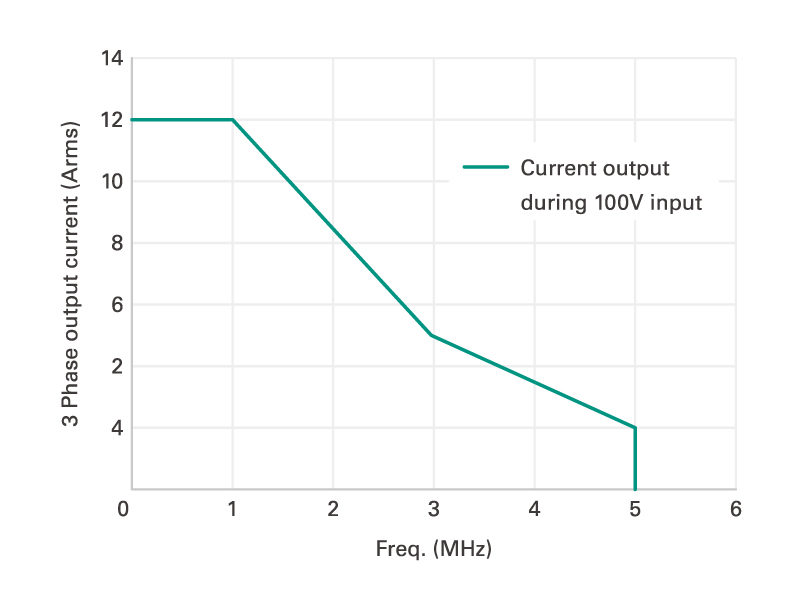
| AC side Max. current | ~12Arms | Derating depending on the switching frequency |
| AC side rated power | 4kVA | |
| Switching frequency | ~5MHz | |
| Dead-time | 30 ns over | Dead time generation function is not mounted. Arm short-circuit prevention function is mounted. |
| Voltage sensor circuit | 400V / 4V | ・P-N terminal voltage ・Gate block when OV or UV is applied ・Protection threshold is adjustable with volume |
| Current sensor circuit | ±50A / ±4V | ・Three-phase current ・Gate block on OC (peak) ・Protection threshold is adjustable with volume |
| Control power enter 5V | 0.6A max | |
| Control Power Enter 24V | 0.8A max |
External interface
| Gating signal | Input | 5V TTL / Negative logic / Pulled up of 4.7 kΩ at input side |
|---|---|---|
| Error reset Signal | Input | 5V TTL / Negative logic (low at reset) / Pulled up of 4.7 kΩ at input side |
| Error signal | Output | 5V TTL / Negative logic (low in error) / Protection detection output |
| Analog signal | Output | DC voltage sensor 1 point / AC current sensors 3 points |
| Error signal (Error link function) |
Input/Output | 5V TTL / Positive logical / Share error information |
| Reset-signal (Error link function) |
Input/Output | 5V TTL / Positive logical / Share reset information |
Derating
-
Block Diagram